
The AI Chip War: Can Google’s TPU Overthrow NVIDIA’s GPU Dominance with a Cost Revolution?
[This article may contain PR]
An enormous tectonic shift is underway in the AI industry. The long-standing fortress of NVIDIA, the undisputed king of AI chips, is finally showing cracks. The epicenter of this shake-up is the Tensor Processing Unit (TPU), an AI-specific chip custom-developed by Google.
We are even seeing market sentiment show an inverse correlation, with Google’s stock price climbing as NVIDIA’s dips. Crucially, major companies leading the AI frontier—including Meta, OpenAI, and Anthropic—are actively considering or implementing Google’s TPU to reduce their reliance on NVIDIA. This development is fueling massive anticipation that the era of “NVIDIA sole dominance” in the AI chip market may be drawing to a close.
This intensifying competition provides significant benefits for AI developers: substantial cost reduction and improved performance. Whether you are a regular user of ChatGPT or Gemini, or a business planning AI adoption, understanding how the TPU is changing the AI landscape is crucial for comprehending the future of technology.
This article will provide a clear, jargon-free explanation of Google TPU, the force poised to fundamentally restructure the AI industry. We will explore why it is more efficient than the Graphics Processing Unit (GPU), and whether the rise of the TPU truly spells the end of NVIDIA’s dominance.

- The Defining Difference: Why TPU Challenges NVIDIA’s GPU Hegemony
- NVIDIA’s Moat: The CUDA Ecosystem Barrier
- The TPU Advantage: Unbeatable Cost, Power Efficiency, and Scale
- Will NVIDIA’s Reign End? The Short-Term Outlook
- The Game Changer: Fundamentals of the Google TPU
- Where is the TPU Used Today? Meta, OpenAI, and Anthropic’s Strategy
- TPU Powering Google’s Internal Services
- External Provisioning and the Strategies of Meta, OpenAI, and Anthropic
- The Production Pipeline: Who Builds the TPU? (TSMC and Broadcom’s Role)
- The Future of TPU: Can It Shatter NVIDIA’s Fortress Completely?
- The Greatest Barrier to TPU Adoption: The Fear of Vendor Lock-in
- The Evolution of the AI Market and TPU’s Opportunity
- Conclusion: The AI Competition and the Path to NVIDIA Diversification
The Defining Difference: Why TPU Challenges NVIDIA’s GPU Hegemony
While both GPU and TPU accelerate AI computations, they differ decisively in architecture, versatility, and ecosystem, which is the core of the Google vs. NVIDIA competition.
The GPU was originally designed for 3D game graphics. As a general-purpose accelerator, it boasts versatility to handle all parallel computing tasks, including image processing, simulations, and financial calculations. However, when performing only AI-specific calculations, the GPU carries “architectural baggage”—unused circuitry meant for graphics—which consumes power and space, leading to poor energy efficiency.
In contrast, the TPU is an Application-Specific Integrated Circuit (ASIC) designed from the ground up to specialize exclusively in AI (matrix arithmetic). By stripping away all unnecessary components, such as graphics features, the TPU achieves unrivaled efficiency for specific AI tasks.
NVIDIA’s Moat: The CUDA Ecosystem Barrier
The main reason NVIDIA holds a 90%+ share and maintains its dominant position in the AI chip market is not just superior GPU performance, but the powerful CUDA software ecosystem built over two decades.
The Global Software Standard: Nearly all AI workloads are developed on the CUDA platform, making it the “native language” for AI engineers.
The High Switching Cost: If a company chooses to migrate from GPUs to an ASIC like the TPU, they might need to rewrite millions of lines of code. This high barrier to entry—the lack of flexibility and ease of migration—is NVIDIA’s impenetrable “fortress” and the biggest obstacle for the TPU’s mass adoption. NVIDIA counters the TPU threat by emphasizing that its chips offer ” higher performance, versatility, and interchangeability ” than application-specific chips, leveraging their general-purpose nature as their primary defense.
The TPU Advantage: Unbeatable Cost, Power Efficiency, and Scale
The reason the Google TPU still poses a credible threat to NVIDIA’s stronghold is its astonishing cost and power efficiency in both inference and training.
Meta’s primary motivation for considering TPU adoption is the significant economic benefit: an anticipated 30% to 50% cost reduction compared to NVIDIA’s highest-performing GPUs. Furthermore, the TPU v4 ecosystem is highly power-efficient, potentially cutting CO2 emissions by half compared to other contemporary specialized hardware. The newest TPU, “Trillium” (v6e), is reported to be 67% more energy-efficient than its predecessor, making it vital for sustainably scaling massive AI infrastructure.
Moreover, Google’s TPU excels due to its proprietary interconnect technology that enables large-scale parallel computing. Google’s Optical Circuit Switch (OCS) allows thousands of TPUs to be flexibly connected, enabling a cluster of 9,216 TPUs to function as one colossal supercomputer, offering a level of scalability that may surpass NVIDIA’s systems.
Will NVIDIA’s Reign End? The Short-Term Outlook
(Source: Google)
In the short term, NVIDIA’s monopoly is expected to continue. NVIDIA has built a multi-layered fortress based on chip performance, the CUDA ecosystem, and supply chain dominance, securing most of TSMC’s manufacturing capacity.
However, the diversification of the market is certain in the medium to long term. By serving the emerging AI need for high-efficiency, low-cost processing of standardized, large-scale workloads—such as LLM training, inference, and recommendation systems—the TPU will gradually chip away at NVIDIA’s market share. This signals a shift toward a “multi-source strategy” era, where GPUs (the general-purpose factory) and TPUs/ASICs (the specialized line) coexist and divide labor.
The Game Changer: Fundamentals of the Google TPU
The Google TPU (Tensor Processing Unit) is an AI accelerator custom-developed by Google to speed up machine learning workloads. It is a type of Application-Specific Integrated Circuit (ASIC).
TPU development began in response to a “critical situation” where conventional hardware could not keep pace with the massive computational demands of AI. Around 2013, Google estimated that if every Android user utilized voice search for just three minutes a day, the company would need to double the number of computers in its data centers. To solve this, the TPU was born: a specialized chip focused purely on AI calculations.
Google started using the TPU internally in 2015, and it remains the core engine powering all of Google’s AI-powered applications that serve over a billion users, including Google Search, Google Photos, Google Translate, and Google Assistant.
The TPU Difference: Domain-Specific Architecture
The TPU’s innovation lies in its design philosophy. While CPUs and GPUs are general-purpose “jacks-of-all-trades,” the TPU is a “master” that has perfected the single path of neural network computation. This “domain-specific architecture” is the true game-changer.
TPUs are optimized to accelerate two primary AI workloads: training AI models and running (inference) those trained models.
- Training: This is the labor-intensive, initial process of teaching AI knowledge using massive datasets. TPUs are highly optimized for training large, complex Deep Learning Models and Large Language Models (LLMs).
- Inference: This is the ongoing, continuous task of using trained knowledge. TPUs are particularly noteworthy for delivering unmatched cost efficiency and processing speed during inference.
The core technology of the TPU is the Systolic Array. This mechanism functions like a perfectly synchronized factory assembly line, where thousands of simple calculators process data and computations rhythmically. By dramatically reducing round trips to memory—which CPUs and GPUs typically do after every calculation—the TPU achieves overwhelming efficiency.
The original TPU (V1) recorded staggering figures: 15x to 30x the performance and 30x to 80x the power efficiency compared to contemporary CPUs and GPUs.
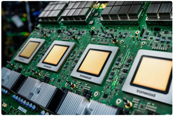
The latest TPU, “Ironwood” (TPU v7), boasts a peak computation performance of 4,614 TFLOP/s per chip. This level of power is capable of running ultra-large AI models and delivering instant responses to all users of AI services.

Where is the TPU Used Today? Meta, OpenAI, and Anthropic’s Strategy
For a long time, the Google TPU was exclusively used for Google’s internal workloads. However, in recent years, external leasing through the Google Cloud Platform (GCP) has accelerated, leading major AI industry players to consider or begin adoption.
TPU Powering Google’s Internal Services
Google powers all its major AI-enabled applications—including Search, Gemini, and Waymo—with TPUs. Crucially, Google is developing its cutting-edge models without purchasing NVIDIA GPUs for its own AI workloads.
- Gemini: Google’s state-of-the-art AI model, “Gemini 3 Pro,” was trained exclusively using Google’s TPUs. This proves that TPUs can deliver performance comparable to, or even exceeding, GPUs for large-scale AI training, raising a red flag for NVIDIA.
External Provisioning and the Strategies of Meta, OpenAI, and Anthropic
Reports indicate that Google is negotiating the large-scale sale of the TPU chips themselves to major companies like Meta and Apple.
- Meta: Meta is reportedly engaged in multi-billion-dollar negotiations to utilize Google TPUs in its data centers starting in 2027. Meta values the TPU’s high performance and promised 30% to 50% cost savings for training its recommendation systems.
- Anthropic: Anthropic, the developer of the competing LLM “Claude,” is partnering with Google and planning to lease up to one million TPUs. Anthropic demonstrates a clear division of labor, using Google TPUs for routine inference tasks, highlighting the cost-effectiveness and processing power of the TPU for inference.
- OpenAI: OpenAI, the creator of ChatGPT, has also begun utilizing Google TPUs. Their objectives are cost reduction to mitigate NVIDIA’s high chip prices and to achieve multi-cloud capability. However, Google appears to be monopolizing its latest TPU generation internally, providing OpenAI with previous-generation models.
The adoption of TPUs by top-tier AI companies creates a potential “domino effect” that challenges NVIDIA’s sole control, fostering healthy dispersion of AI investment and competition.
The Production Pipeline: Who Builds the TPU? (TSMC and Broadcom’s Role)
(Source: TSMC)
Google handles the architectural design and specifications for the TPU, while Broadcom and TSMC (Taiwan Semiconductor Manufacturing Company) are deeply involved in the manufacturing process.
The Google-Broadcom Alliance
While Google owns the intellectual property (IP) for the TPU, Broadcom serves as a co-developer in the manufacturing effort. Broadcom is responsible for translating Google’s designs into manufacturable silicon, overseeing the ASIC design, and managing the chip’s fabrication and packaging through third-party foundries like TSMC.
Google maximizes cost control by handling the chip’s “brain” (front-end design) internally and assigning only the physical placement to Broadcom. This strategy minimizes margins paid to partners, gaining a competitive edge by avoiding the significant profits currently funneled to NVIDIA.
TSMC Capacity and the NVIDIA Supply Chain Hurdle
TPU manufacturing is outsourced to foundries like TSMC, similar to NVIDIA. However, TSMC’s production capacity is currently a major constraint in AI chip manufacturing. NVIDIA holds a strategic advantage by having secured nearly all of TSMC’s available capacity for its own chip production. If Google attempts to sell TPUs on a scale of millions of units, the supply constraint remains a major challenge to overcoming NVIDIA’s dominance.
The Future of TPU: Can It Shatter NVIDIA’s Fortress Completely?
The introduction of the Google TPU created a “significant crack” in NVIDIA’s monopoly, but its future depends on the barriers to adoption and the evolutionary path of the AI chip market.
The Greatest Barrier to TPU Adoption: The Fear of Vendor Lock-in
For the TPU to achieve global adoption comparable to the GPU, it must overcome several major obstacles:
- The CUDA Ecosystem: The NVIDIA CUDA software foundation, which AI developers have used for decades, cannot be easily replaced.
- Cloud Restriction and Lock-in: While NVIDIA GPUs can be leased on any cloud (AWS, Azure, GCP), TPUs are primarily restricted to Google Cloud (GCP). Companies fear “vendor lock-in”—the risk of being trapped if Google drastically increases TPU usage fees. Consequently, many tend to choose NVIDIA, paying a premium for versatility and freedom.
NVIDIA CEO Jensen Huang strongly argues that NVIDIA offers ” higher performance, versatility, and interchangeability ” compared to ASICs like the TPU, which are “designed for specific AI frameworks,” thus using the TPU’s specialization as a means to maintain their advantage.
The Evolution of the AI Market and TPU’s Opportunity
However, the direction of the AI chip market evolution presents a major opportunity for the TPU.
The Expansion of the Inference Market: While the AI training market is predicted to eventually saturate, the inference market (daily execution) is expected to become vastly larger than the training market. In the inference phase, speed and cost efficiency are paramount, maximizing the utility of the TPU’s superior cost-performance ratio.
TPU Performance Evolution: The latest “Ironwood v7” TPU is reaching a level of single-chip performance that is on par with NVIDIA’s newest GPUs, featuring the same memory capacity as NVIDIA’s Blackwell B200: 192GB of HBM.
Google is reportedly holding internal discussions that will determine the company’s future: whether to use the TPU as a proprietary “secret weapon” to enhance GCP’s competitiveness, or to pivot toward external sales, establishing itself as a standalone AI chip manufacturer.
Conclusion: The AI Competition and the Path to NVIDIA Diversification
The arrival of the Google TPU and its adoption by major companies have broken NVIDIA’s sole dominance, driving competition and innovation in the AI industry.
The TPU is a specialized chip born from Google’s survival strategy: it achieves unmatched cost and power efficiency by processing AI computations on a dedicated assembly line (Systolic Array), shedding the “architectural baggage” associated with the GPU’s general-purpose design.
The motivation for top AI firms like Meta, Anthropic, and OpenAI to adopt the TPU is clear economic rationale: moving away from NVIDIA’s high chip costs and executing specific workloads, like inference processing, with high efficiency and lower expense. This trend indicates a transition to a “multi-source strategy” era, where AI infrastructure will rely on a hybrid fleet of GPUs (general-purpose) and TPUs/ASICs (specialized).
NVIDIA’s CUDA ecosystem remains a strong “moat,” and the TPU will not fully replace the GPU in the near future. However, in a future where the AI inference market expands exponentially, the TPU’s cost and efficiency advantage will secure Google a long-term competitive edge.
The AI industry will accelerate toward further technological innovation, driven by this “clash of titans” between NVIDIA and Google. This competition promises significant benefits for AI users: the creation of faster, cheaper, and more powerful AI services.


What is Cerebras Systems? The Wafer-Scale AI Chip Challenging NVIDIA’s Inference Dominance
Google TurboQuant Explained: How the New AI Memory Algorithm Slashes Costs and Disrupts Semiconductor Stocks
What is Physical AI? The 2026 Trend That Will Revolutionize Robotics and Daily Life
Rapidus Explained: Japan’s Bold $35B Bet on 2nm Chips to Rival TSMC
Can Former PlayStation Engineers Dethrone NVIDIA? Meet the Japanese AI Chip Slashing Power Use by 90%
Google Mixboard: Visualize Ideas Fast with Nano Banana
On the lifestyle web magazine "Minna no Rakuraku Magazine",
we update useful tips and deals every month. Please bookmark us!
- Puppet Sunsun: Who Is the “Screaming Blue Thing” and Is He Related to Elmo?
- ChatGPT’s “Code Red” Update: GPT-5.2 Release Date, Pricing, and Gemini 3 Comparison