

Can Former PlayStation Engineers Dethrone NVIDIA? Meet the Japanese AI Chip Slashing Power Use by 90%
【この記事にはPRを含む場合があります】
While the world marvels at the rapid evolution of Generative AI like ChatGPT and Gemini, a silent crisis is brewing in the background: the staggering energy consumption of the data centers powering these models. As the tech industry grapples with an ongoing NVIDIA GPU shortage and soaring electricity costs, a group of legendary engineers from Japan is stepping up with a potential game-changer.
The team behind the iconic hardware of the PlayStation 2 and PlayStation 3 has reunited to tackle AI’s biggest bottleneck. Their weapon? A revolutionary new chip architecture called CGLA, which claims to reduce power consumption by a staggering 90% compared to traditional NVIDIA GPUs.
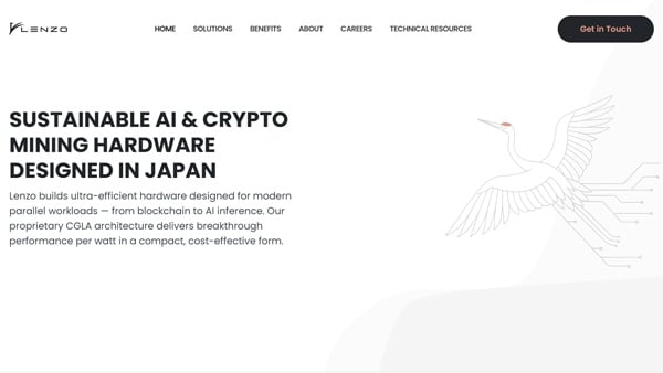
In this article, we’ll dive into the technology developed by the Japanese startup LENZO, explore how CGLA differs from current industry standards like Google’s TPU, and see how it might reshape the future of artificial intelligence.

- What is CGLA? The "Dream Team" Reinventing AI Efficiency
- The Secret to 90% Energy Savings: Stopping the "Data Commute"
- CGLA vs. NVIDIA GPU vs. Google TPU: The "Goldilocks" Solution
- Future-Proofing for the Post-Transformer Era
- The Road Ahead: Overcoming the "CUDA" Moat
- A New Chapter for Japanese Innovation
What is CGLA? The “Dream Team” Reinventing AI Efficiency
(Source: Lenzo)
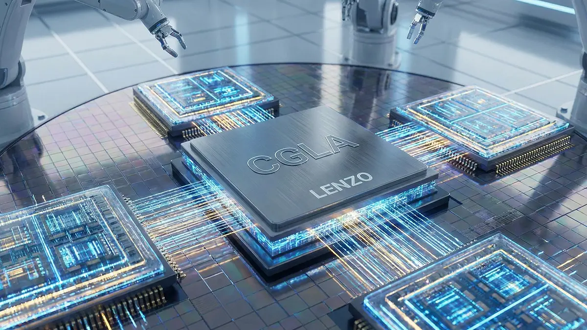
CGLA stands for Coarse Grained Linear Array. It is a novel architecture designed from the ground up to maximize AI processing efficiency.
The startup behind this breakthrough, LENZO, is led by a “dream team” of Japanese engineering. The roster includes the veteran designers of the PlayStation’s core CPUs and supercomputer experts from Fujitsu. These engineers are now applying their decades of experience—honed by squeezing every drop of performance out of gaming consoles—to solve the energy crisis in AI.
The Secret to 90% Energy Savings: Stopping the “Data Commute”
The primary reason current AI chips consume so much power isn’t actually the “calculating” itself—it’s the moving of data. Research from NVIDIA shows that moving data just 1mm within a chip consumes more energy (26 picojoules) than the actual computation (20 picojoules).
Traditional CPUs and GPUs use what is known as the “von Neumann architecture,” where the processing unit and memory are separate.
Think of it like a kitchen:
- The Processor is your cutting board.
- The Memory is your refrigerator.
In current chips, every time the “cook” needs to chop a vegetable, they have to walk all the way to the fridge and back. This constant commuting wastes an incredible amount of energy.
CGLA changes the game by using a “data-flow” model. Instead of separate units, CGLA aligns processing units and small memory cells in a linear row. Data flows like a bucket brigade: as soon as one person finishes their task, they hand it to the person right next to them. By physically minimizing the distance data must travel, CGLA virtually eliminates the “commute,” resulting in drastic power savings.
CGLA vs. NVIDIA GPU vs. Google TPU: The “Goldilocks” Solution
How does CGLA stack up against the titans of the industry?
- NVIDIA GPU: Flexible but Power-Hungry. GPUs are the versatile “all-rounders” of the AI world. They can handle almost any task, but their general-purpose nature leads to the “von Neumann bottleneck,” consuming massive amounts of power. It’s often compared to using a sledgehammer for delicate surgery.
- Google TPU: Efficient but Rigid. Google’s Tensor Processing Unit (TPU) is highly specialized for AI matrix math, moving data like a conveyor belt (Systolic Array). It’s very fuel-efficient but “inflexible”—it’s built for specific calculations and can’t easily adapt if AI models change.
- CGLA: The Best of Both Worlds. CGLA aims to provide the efficiency of a TPU with the flexibility of a GPU. Its defining feature is being “Configurable”—meaning the internal circuitry can be reprogrammed via software to optimize for different AI models.
Future-Proofing for the Post-Transformer Era
The AI landscape moves at lightning speed. While “Transformers” (the tech behind GPT) are the current standard, new models like “Mamba” are already emerging.
Because CGLA is software-configurable, it doesn’t become obsolete when a new AI architecture debuts. Engineers can simply “rewire” the chip’s internal logic to handle new types of math. This longevity gives it a significant edge over traditional fixed-function ASIC chips.
The Road Ahead: Overcoming the “CUDA” Moat
The biggest challenge for LENZO isn’t the hardware—it’s CUDA. NVIDIA has built a massive software ecosystem that AI developers rely on. To break through, LENZO plans to target specific markets first, such as inference servers in data centers (where power costs are the #1 concern) and crypto mining.
As global cloud providers look for ways to reduce their dependency on NVIDIA and slash their carbon footprints, CGLA emerges as a powerful alternative.

A New Chapter for Japanese Innovation
LENZO’s mission goes beyond just cost-cutting; it’s about solving a global energy problem. With manufacturing plans at TSMC already in motion, this technology is nearing commercial reality.
Japan was once the undisputed king of semiconductors. Now, led by the veterans who defined the golden age of gaming, the country is ready for a counteroffensive in the AI era. Keep an eye on CGLA—it might just be the architecture that keeps the AI revolution sustainable.

- Why KFC Spain’s Twitter is Unhinged: The Genius Behind the Chaos & Anime Memes
- Hooked on Anger: Why 'Rage Bait' Is 2025's Word of the Year (And How to Escape It)